A team of scientists at Google has used AI to design physical layouts of computer chips superior to those created by humans, in a major breakthrough, a new paper published in Nature reveals.
The AI-built chip "floorplans" are no cloistered academic curiosity: the method was used to support the design of new Google tensor processing units (TPUs) -- or chips deployed to accelerate machine learning workloads.
Using deep reinforcement learning, a research team led by Google's Azalia Mirhoseini and Anna Goldie generated chip "floorplans" that are "superior or comparable to those produced by humans in all key metrics, including power consumption, performance and chip area", the June 9 paper reveals.
The results could be far-reaching: "Automating and accelerating the chip design process can enable co-design of AI and hardware, yielding high-performance chips customized to important workloads, such as autonomous vehicles, medical devices and data centres," the research team notes.
The method saw superior designs generated in just six hours. The breakthrough is so significant that Andrew Kahng, a world-leading chip expert and professor of computer science at UC San Diego suggested in a companion comment piece in Nature that the innovation may yet keep Moore’s law alive.
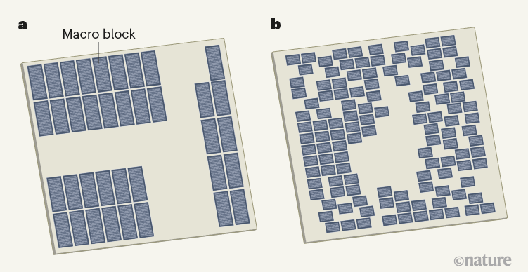
What is chip floorplanning?
Microchip floorplans designed by humans (left) vs those produced by a machine-learning system. Credit: Nature.
Computer chips are divided into numerous individual modules, e.g. memory subsystems, compute units or control logic systems, with these cells and macro blocks interconnected up to 30 miles of interconnect wires.
As Google's Mirhoseini and Goldie et al note: "These blocks can be described by a netlist, a hypergraph of circuit components, such as macros (memory components) and standard cells (logic gates such as NAND, NOR and XOR), all of which are connected by wires. Chip floorplanning involves placing netlists onto chip canvases (two-dimensional grids) so that performance metrics (for example, power consumption, timing, area and wirelength) are optimized, while adhering to hard constraints on density and routing congestion."
As Kahng emphasises: "Given this staggering complexity, the chip-design process itself is another miracle — in which the efforts of engineers, aided by specialized software tools, keep the complexity in check.
"The locations of cells and macro blocks in the chip are crucial to the design outcome. Their placement determines the distances that wires must span, and thus affects whether the wiring can be successfully routed between components and how quickly signals can be transmitted between logic gates. Optimization of chip placement has been extensively studied for at least six decades. Seminal innovations in the mathematical field of applied optimization, such as a method known as simulated annealing, have been motivated by the challenge of chip placement..."
AI chip design
Typically human physical designers must iterate for months with commercial electronic design automation (EDA) tools. This involves "taking as input a register transfer level (RTL) description of the chip netlist, generating a manual placement of that netlist onto the chip canvas, and waiting up to 72 hours for EDA tools to evaluate that placement."
By contrast, the papers authors trained a deep neural network agent that can successfully place macro blocks into a chip layout by applying its strategy (generated using reinforcement learning) to identify the best ‘action’ — that is, where to place the next block.
As the report details, when the RL agent is pre-trained on a set of 10,000 different chip floorplans, it is already successful when used in a ‘one shot’ mode on a new design: but with just six extra hours of fine-tuning, it can produce floorplans that are superior to those developed by human experts for existing chips. It is trained to respond to the "rewards" of optimised wirelength, routing congestion, density, power, timing and area
The breakthrough has the "potential to save thousands of hours of engineering effort for each next generation ASIC", Mirsoeni noted on Twitter, adding that "we envision a future where we will use similar techniques to automatically co-optimize across the stack (from Architecture to Place&Route), producing more efficient custom chips faster and cheaper. Our techniques also apply to other placement problems such as those that appear in FPGAs, PCB design, and city planning."
The full reinforcement learning methodology is detailed in their article in Nature which you can read, sans paywall, here. See Professor Andrew B. Kahng's view is, here.